Written by Colin Riley, an Engineer and Writer at Domipheus Labs
This part of a series of posts detailing the steps and learning undertaken to design and implement a CPU in VHDL. You can find more articles from Colin on his blog via http://labs.domipheus.com/blog/. To read more from this series, click here.
For those who follow me on twitter, you’ll have seen my recent tweets regarding Zephyr OS running on RPU. This was a huge amount of work to get running, most of it debugging on the FPGA itself. For those new to FPGA development, trying to debug on-chip can be a very difficult and frustrating experience. Generally, you want to debug in the simulator – but when potential issues are influenced by external devices such as SD cards, timer interrupts, and hundreds of millions of cycles into the boot process of an operating system – simulators may not be feasible.
Blog posts on the features I added to RPU to enable Zephyr booting, such as proper interrupts, exceptions and timers are coming – but it would not have been possible without a feature of the RPU SoC I have not yet discussed.
CPU Tracing
Most real processors will have hardware features built in, and one of the most useful low-level tools is tracing. This is when at an arbitrary time slice, low level details on the inner operation of the core are captured into some buffer, before being streamed elsewhere for analysis and state reconstruction later.
Note that this is a one-way flow of data. It is not interactive, like the debugging most developers know. It is mostly used for performance profiling but for RPU would be an ideal debugging aid.
Requirements
For the avoidance of doubt; I’m defining “A Trace” to be one block of valid data which is dumped to a host PC for analysis. For us, dumping will be streaming the data out via UART to a development PC. Multiple traces can be taken, but when the data transfer is initiated, the data needs to be a real representation of what occurred immediately preceding the request to dump the trace. The data contained in a trace is always being captured on the device in order that if a request is made, the data is available.
These requirements require a circular buffer which is continually recording the state. I’ll define exactly what the data is later – but for now, the data is defined as 64-bits per cycle. Plenty for a significant amount of state to be recorded, which will be required in order to perform meaningful analysis. We have a good amount of block rams on our Spartan 7-50 FPGA, so we can dedicate 32KB to this circular buffer quite easily. 64-bits into 32KB gives us 4,096 cycles of data. Not that much you’d think for a CPU running at over 100MHz, but you’d be surprised how quickly RPU falls over when it gets into an invalid state!
It goes without saying that our implementation needs to be non-intrusive. I’m not currently using the UART connected to the FTDI USB controller, as our logging output is displayed graphically via a text-mode display over HDMI. We can use this without impacting existing code. Our CPU core will expose a debug trace bus signal, which will be the data captured.
We’ve mentioned the buffer will be in a block ram; but one aspect of this is that we must be wary of the observer effect. This issue is very much an issue for performance profiling, as streaming out data from various devices usually goes through memory subsystems which will increase bandwidth requirements, and lead to more latency in the memory operations you are trying to trace. Our trace system should not effect the execution characteristics of the core at all. As we are using a development PC to receive the streamed data, we can completely segregate all data paths for the trace system, and remove the block ram from the memory mapped area which is currently used for code and data. With this block ram separate, we can ensure it’s set up as a true dual port ram with data width the native 64bit. One port will be for writing data from the CPU, on the CPU clock domain. The second port will be used for reading the data out at a rate which is dictated by the UART serial baud – much, much, slower. Doing this will ensure tracing will not impact execution of the core at any point, meaning our dumped data is much more valuable.
Lastly, we want to trigger these dumps at a point in time when we think an issue has occurred. Two immediate trigger types come to mind in addition to a manual button.
- Memory address
- Comparison with the data which is to be dumped; i.e, pipeline status flags combined with instruction types.
Implementation
The implementation is very simple. I’ve added a debug signal output to the CPU core entity. It’s 64 bits of data consisting of 32 bits of status bits, and a 32-bit data value as defined below.
This data is always being output by the core, changing every cycle. The data value can be various things; the PC when in a STAGE_FETCH state, the ALU result, the value we’re writing to rD in WRITEBACK, or a memory location during a load/store.
We only need two new processes for the system:
- trace_streamout: manages the streaming out of bytes from the trace block ram
- trace_en_check: inspects trigger conditions in order to initiate a trace dump which trace_streamout will handle
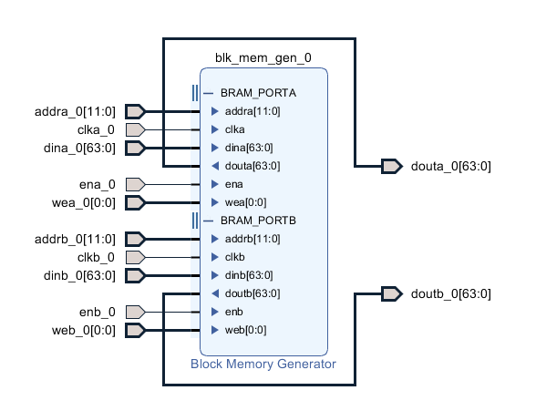
The BRAM used as the circular trace buffer is configured as 64-bits word length, with 4096 addresses. It was created using the Block Memory Generator, and has a read latency of 2 cycles.
We will use a clock cycle counter which already exists for dictating write locations into the BRAM. As it’s used as a circular buffer, we simply take the lower 12 bits of the clock counter as address into the BRAM.
Port A of the BRAM is the write port, with it’s address line tied to the bits noted above. It is enabled by a signal only when the trace_streamout process is idle. This is so when we do stream out the data we want, it’s not polluted with new data while our slow streamout to UART is active. That new data is effectively lost. As this port captures the cpu core O_DBG output, it’s clocked at the CPU core clock.
Port B is the read port. It’s clocked using the 100MHz reference clock (which also drives the UART – albeit then subsampled via a baud tick). It’s enabled when a streamout state is requested, and reads an address dictated by the trace_streamout process.
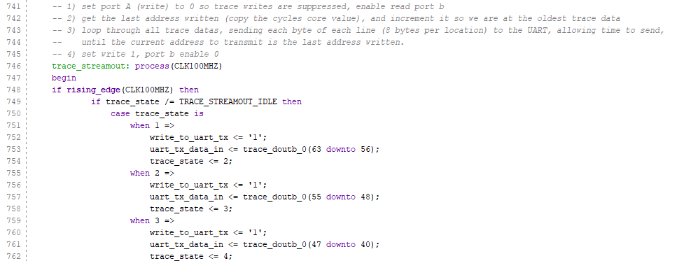
The trace_streamout process, when the current streamout state is idle, checks for a dump_enable signal. Upon seeing this signal, the last write address is latched from the lower cycle counter 12 bits. We also set a streamout location to be that last write +1. This location is what is fed into Port B of the BRAM/ circular trace buffer. When we change the read address on port B, we wait some cycles for the value to properly propagate out. During this preload stall, we also wait for the UART TX to become ready for more data. The transmission is performed significantly slower than the clock that trace_streamout runs at, and we cannot write to the TX buffer if it’s full.
The UART I’m using is provided by Xilinx and has an internal 16-byte buffer. We wait for a ready signal as then we know that writing our 8 bytes of debug data (remember, 64-bit) quickly into the UART TX will succeed. In addition to the 8 bytes of data, I also send 2 bytes of magic number data at the start of every 64-bit packet as an aid to the receiving logic; we can check the first two bytes for these values to ensure we’re synced correctly in order to parse the data eventually.
After the last byte is written, we increment our streamout location address. If it’s not equal to the last write address we latched previously, we move to the preload stall and move the next 8 bytes of trace data out. Otherwise, we are finished transmitting the entire trace buffer, so set out state back to idle and re-enable new trace data writes.
Triggering streamout
Triggering a dump using dump_enable can be done a variety of ways. I have a physical push-button on my Arty S7 board set to always enable a dump, which is useful to know where execution currently is in a program. I have also got a trigger on reading a certain memory address. This is good if there is an issue triggering an error which you can reliably track to a branch of code execution. Having a memory address in that code branch used as trigger will dump the cycles leading up to that branch being taken. There are one other types of trigger – relying on the cpu O_DBG signal itself, for example, triggering a dump when we encounter an decoder interrupt for an invalid instruction.
I hard-code these triggers in the VHDL currently, but it’s feasible that these can be configurable programmatically. The dump itself could also be triggered via a write to a specific MMIO location.
Parsing the data on the Debug PC
The UART TX on the FPGA is connected to the FTDI USB-UART bridge, which means when the FPGA design is active and the board is connected via USB, we can just open the COM port exposed via the USB device.
I made a simple C# command line utility which just dumps the packets in a readable form. It looks like this:
| 12345678910 | [22:54:19.6133781]Trace Packet, 00000054, 0xC3 40 , OPCODE_BRANCH , STAGE_FETCH , 0x000008EC INT_EN , :[22:54:19.6143787]Trace Packet, 00000055, 0xD1 40 , OPCODE_BRANCH , STAGE_DECODE , 0x04C12083 INT_EN , :[22:54:19.6153795]Trace Packet, 00000056, 0xE1 40 , OPCODE_LOAD , STAGE_ALU , 0x00000001 INT_EN , :[22:54:19.6163794]Trace Packet, 00000057, 0xF1 C0 , OPCODE_LOAD , STAGE_MEMORY , 0x0000476C REG_WR INT_EN , :[22:54:19.6183798]Trace Packet, 00000058, 0x01 C0 , OPCODE_LOAD , STAGE_MEMORY , 0x0000476C REG_WR INT_EN , :[22:54:19.6183798]Trace Packet, 00000059, 0x11 C0 , OPCODE_LOAD , STAGE_MEMORY , 0x0000476C REG_WR INT_EN , :[22:54:19.6193799]Trace Packet, 00000060, 0x20 C0 , OPCODE_LOAD , STAGE_MEMORY , 0x0000476C REG_WR INT_EN , :[22:54:19.6203802]Trace Packet, 00000061, 0x31 C0 , OPCODE_LOAD , STAGE_MEMORY , 0x0000476C REG_WR INT_EN , :[22:54:19.6213808]Trace Packet, 00000062, 0x43 C0 , OPCODE_LOAD , STAGE_MEMORY , 0x0000476C REG_WR INT_EN , :[22:54:19.6213808]Trace Packet, 00000063, 0x51 C0 , OPCODE_LOAD , STAGE_WRITEBACK , 0x00001CDC REG_WR INT_EN , : |
You can see some data given by the utility such as timestamps and a packet ID. Everything else is derived from flags in the trace data for that cycle.
Later I added some additional functionality, like parsing register destinations and outputting known register/memory values to aid when going over the output.
| 1234 | [22:54:19.6213808]Trace Packet, 00000062, 0x43 C0 , OPCODE_LOAD , STAGE_MEMORY , 0x0000476C REG_WR INT_EN , :[22:54:19.6213808]Trace Packet, 00000063, 0x51 C0 , OPCODE_LOAD , STAGE_WRITEBACK , 0x00001CDC REG_WR INT_EN , :MEMORY 0x0000476C = 0x00001CDCREGISTER ra = 0x00001CDC |
I have also been working on a rust-based GUI debugger for these trace files, where you can look at known memory (usually the stack) and register file contents at a given packet by walking the packets up until the point you’re interested in. It was an excuse to get to know Rust a bit more, but it’s not completely functional and I use the command line C# version more.
The easiest use for this is the physical button for dumping the traces. When bringing up some new software on the SoC it rarely works first time and end up in an infinite loop of some sort. Using the STAGE_FETCH packets which contain the PC I can look to an objdump and see immediately where we are executing without impacting upon the execution of the code itself.
Using the data to debug issues
Now to spoil a bit of the upcoming RPU Interrupts/Zephyr post with an example of how these traces have helped me. But I think an example of a real problem the trace dumps helped solve is required.
After implementing external timer interrupts, invalid instruction interrupts, system calls – and fixed a ton of issues – I had the Zephyr Dining Philosophers sample running on RPU in all it’s threaded, synchronized, glory.
Why do I need invalid instruction interrupts? Because RPU does not implement the M RISC-V extension. So multiply and divide hardware does not exist. Sadly, somewhere in the Zephyr build system, there is assembly with mul and div instructions. I needed invalid instruction interrupts in order to trap into an exception handler which could software emulate the instruction, write the result back into the context, so that when we returned from the interrupt to PC+4 the new value for the destination register would be written back.
It’s pretty funny to think that for me, implementing that was easier than trying to fix a build system to compile for the architecture intended.
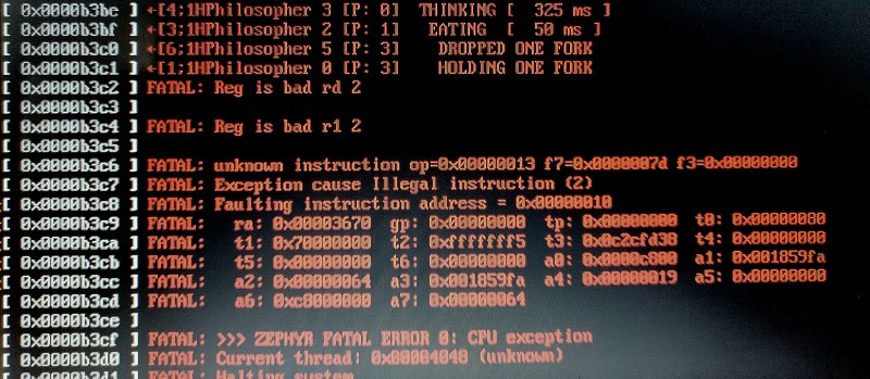
Anyway, I was performing long-running tests of dining philosophers, when I hit the fatal error exception handler for trying to emulate an instruction it didn’t understand. I was able to replicate it, but it could take hours of running before it happened. The biggest issue? The instruction we were trying to emulate was at PC 0x00000010 – the start of the exception handler!
So, I set up the CPU trace trigger to activate on the instruction that branches to print that “FATAL: Reg is bad” message, started the FPGA running, and left the C# app to capture any trace dumps. After a few hours the issue occurred, and we had our CPU trace of the 4096 cycles leading up to the fatal error. Some hundreds of cycles before the dump initiated, we have the following output.
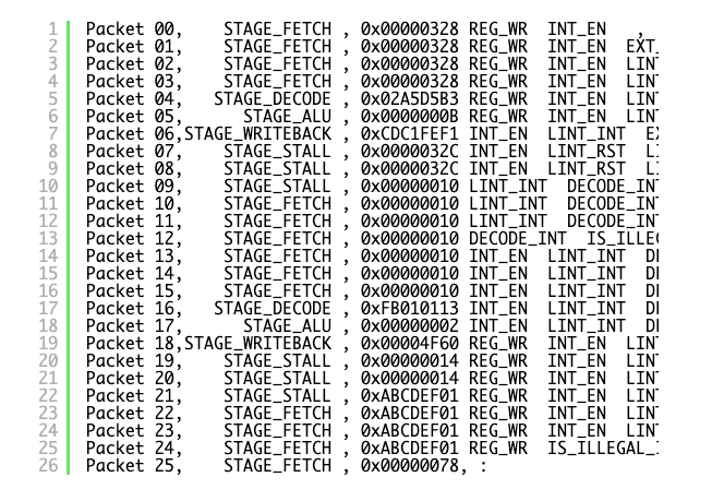
What on earth is happening here? This is a lesson as to why interrupts have priorities 🙂
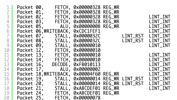
I’ve tried to reduce the trace down to minimum and lay it out so it makes sense. There are a few things you need to know about the RPU exception system which have yet to be discussed:
Each Core has a Local Interrupt Controller (LINT) which can accept interrupts at any stage of execution, provide the ACK signal to let the requester know it’s been accepted, and then at a safe point pass it on to the Control Unit to initiate transfer of execution to the exception vector. This transfer can only happen after a writeback, hence the STALL stages as it’s set up before fetching the first instruction of the exception vector at 0x00000010. If the LINT sees external interrupts requests (EXT_INT – timer interrupts) at the same time as decoder interrupts for invalid instruction, it will always choose the decoder above anything – as that needs immediately handled.
And here is what happens above:
- We are fetching PC 0x00000328, which happens to be an unsupported instruction which will be emulated by our invalid instruction handler.
- As we are fetching, and external timer interrupt fires (Packet 01)
- The LINT acknoledges the external interrupt as there is no higher priority request pending, and signals to the control unit an int is pending LINT_INT (Packet 2)
- As we wait for the WRITEBACK phase for the control unit to transfer to exception vector, PC 0x00000328 decodes as an illegal instruction and DECODER_INT is requested (Packet 5)
- LINT cannot acknowledge the decoder int as the control unit can only handle a single interrupt at a time, and its waiting to handle the external interrupt.
- The control unit accepts the external LINT_INT, and stalls for transfer to exception vector, and resets LINT so it can accept new requests (Packet 7).
- We start fetching the interrupt vector 0x00000010 (Packet 12)
- The LINT sees the DECODE_INT and immediately accepts and acknowledges.
- The control unit accepts the LINT_INT, stalls for transfer to exception vector, with the PC of the exception being set to 0x00000010 (Packet 20).
- Everything breaks, the PC get set to a value in flux, which just so happened to be in the exception vector (Packet 25).
In short, if an external interrupt fires during the fetch stage of an illegal instruction, the illegal instruction will not be handled correctly and state is corrupted.
Easily fixed with some further enable logic for external interrupts to only be accepted after fetch and decode. But one hell is an issue to find without the CPU trace dumps!
Finishing up
So, as you can see, trace dumps are an great feature to have in RPU. A very simple implementation can yield enough information to work with on problems where the simulator just is not viable. With different trigger options, and the ability to customize the O_DBG signal to further narrow down issues under investigation, it’s invaluable. In fact, I’ll probably end up putting this system into any similarly complex FPGA project in the future. The HDL will shortly be submitted to the SoC github repo along with the updated core which supports interrupts.

