Written by Frank Duignan, Electronics Engineer and Lecturer at TU Dublin, Ireland
This is part 2 of a tutorial series by Frank Duignan. Part 1 focused on GPIO – you can read it here.
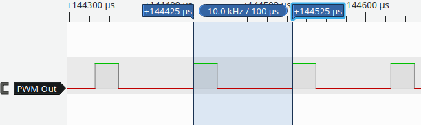
The NRF52833 has a 12 bit, 8 channel Analogue to Digital Converter (ADC) which allows it to convert signals from analogue sensors into numbers that can be used in calculations. The NRF52833 does not have a Digital to Analogue Converter (DAC) (this is quite common for microcontrollers). Instead it fakes an analogue output capability by doing Pulse Width Modulation (PWM) i.e. by sending a square wave to an output pin and varying the percentage time the pin is high. This allows it to control the average output voltage on that pin. A simple RC filter can be used to filter out the pulses and leave a variable output voltage.
Reading an analogue input
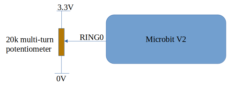
In this example an analogue input is sent to RING0 (there are 5 holes on the Microbit that are designed to accept banana plugs. Ring 0 is the left-most hole when the board is viewed from the speaker side). The RING0 input is connected to Port 0 bit 2 (P0.2) which is also referred to as AIN0 (analogue input 0) in the NRF52833 data sheet. This pin must be configured for operation as an analogue input. This is done using an adc_channel_cfg as shown below.
/*
 * The internal voltage reference is 0.6V
 * The permissable gains are 1/6, 1/5, 1/4, 1/3, 1/2, 1, 2 and 4
 * If a gain of 1/5 is selected then the ADC range becomes 0 to 3V
 */
static const struct device *adc;
// Will read from analog input on P0.2 which is RING 0 on the microbit v2
#define ADC_PORT_BIT 2
struct adc_channel_cfg channel_cfg = {
        /* gain of 1/5 */
        .gain = ADC_GAIN_1_5,
        /* 0.6V reference */
        .reference = ADC_REF_INTERNAL,
        /* sample and hold time of 3us is the default (0 setting) on the NRF52833 */
        .acquisition_time = ADC_ACQ_TIME_DEFAULT,
        /* Channel 0 */
        .channel_id = 0,
        /* AIN0 is specified by setting input_positive to 0+1 i.e. an offset of 1  */
        /* This is as a result of the way the PSELP and PSELN registers work in the NRF52 series of devices */
        /* see page 375 of the NRF52 product specificatoin version : 4452_021 v1.3 */
        .input_positive = 1,
        /* Using single ended conversions */
        .differential = 0
};

int adc_begin()
{
    int ret;
    // Configure the GPIO's
    adc=device_get_binding("ADC_0");
    if (adc == NULL)
    {
        printf("Error acquiring ADC \n");
        return -1;
    }
    ret = adc_channel_setup(adc, &channel_cfg);
    if (ret < 0)
    {
        printf("Error configuring ADC channel 0\n");
        return -2;
    }
    return 0;
}
The NRF52833 can use an internal voltage reference of 0.6V as a basis for ADC conversions as well as fractions of the supply voltage. We will use 0.6V as this is independent of the power supply voltage. Each ADC channel can be scaled by an amplifier. This scaling factor is called “gain” and allows us to control the measurable input voltage range. For example, with a gain of 1 and a voltage reference of 0.6 the ADC will produce its maximum digital output value ((2^12) -1 = 4095) when the input is just 0.6V. If we apply a gain of 1/5 then the measurable input voltage range extends to 3V.
The ADC is of the successive-approximation variety and as such, it requires a stable input voltage during the conversion process. A sample-and-hold circuit (a little capacitor) is used to take a snapshot of the input voltage which is then converted. Capacitors take time to charge and it can happen that insufficient time is allowed for this in which case the snapshot will be different to the actual input voltage at that instant. We can avoid this by allowing a long charging period however this reduces the maximum sampling rate. The acquisition_time field of the adc_channel_config structure allows you control this charging period. It is set to the default of 3 microseconds above.
The channel_id field of the adc_channel_config is used to “name” a particular ADC channel. It is a logical name as opposed to a physical channel in the case of the NRF52833. We associate this adc channel with a particular analogue input using the input_positive field. If we want to use AIN0 this field should be set to ‘1’, for AIN1 this should be 2 etc. i.e. one more than the analogue input channel number as described in the NRF52833 datasheet. The reason for the addition of ‘1’ is to do with the way registers are programmed in this particular microcontroller.
The adc_begin function gets a device structure pointer for the ADC and configures a single channel for use.
To make a reading from the ADC we have to pass an adc_sequence structure to the adc_read
static int16_t channel_0_data;  // This will hold the adc result

struct adc_sequence sequence = {
        /* This is a bitmask that tells the driver which channels to convert : bit n = 1 for channel n */
        .channels    = (1 << 0),
        /* Where will the data be stored (could be an array if there are multiple channels to convert */
        .buffer      = &channel_0_data,
        /* buffer size in bytes, not number of samples */
        .buffer_size = sizeof(channel_0_data),
        /* 12 bit resolution */
        .resolution  = 12,
        /* nulls for the rest of the fields */
        .options = NULL,
        .calibrate = 0,
        .oversampling = 0,
};
int adcread()
{
    int ret;
    ret = adc_read(adc, &sequence);
    return channel_0_data;
}
In our case we are doing a sequence of 1 conversion so a single 16 bit result is stored to the channel_0_data variable. The address and size of an array can be passed here instead if multiple samples are to be taken.
Analogue output
static const struct device *pwm;
int pwm_begin()
{
    int ret;
    // Configure the GPIO's
    pwm=device_get_binding("PWM_0");
    if (pwm == NULL)
    {
        printf("Error acquiring PWM interface \n");
        return -1;
    }
    return 0;
}
int pwm_write(uint16_t value)
{

    return pwm_pin_set_usec(pwm,3,PWM_PERIOD_US,value,0);
}
The pwm_begin function acquires a pointer to the device structure for the PWM_0 device. The pwm_write function takes a single argument which is the number of microseconds the associated output pin should be high in each PWM cycle. The constant PWM_PERIOD_US in this example is set to 100 so the incoming parameter to this function should be in the range 0 to 100. The pwm_pin_set_usec function takes 5 arguments:
A pointer to the PWM device structure
The pin number that is to be controlled
The PWM period expressed in microseconds
The PWM high-time expressed in microseconds
A “flags” value which can be used to set the PWM output polarity (0 works fine here)
I have chosen to use P0.3 as the PWM output pin. This is connected to RING1 on the BBC microbit which makes it easy to use with banana plugs. The PWM output can be routed to other pins but I have found that not all of them work (probably due to being configured for use with other peripherals by the OS).
The app.overlay file.
The analogue input and output routines shown above require an additional file be created in the project directory: app.overlay. This file can override and add to settings in the default device tree (dts) file for this device which is to be found in zephyr/boards/arm/bbc_microbit_v2/bbc_microbit_v2.dts. In this file, the adc and pwm devices are disabled. Also, there are no pins assigned to the PWM subsystem. We can fix all of this with the following app.overlay file:
&adc {
    status = "okay";
};
&pwm0 {
    status = "okay";
    ch
Putting it all together
The following main function reads a value from the ADC and writes a proportional value to the PWM system. The average output voltage should therefore track the input voltage (it will be a little higher because the output switches between 0 and 3.3V. If the input voltage is 3V then the duty will be 100% resulting in an output voltage of 3.3V).
void main(void)
{
    int ret;
    ret = adc_begin();
    if (ret < 0)
    {
        printf("\nError initializing adc.  Error code = %d\n",ret);
        while(1);
    }
    ret = pwm_begin();
    if (ret < 0)
    {
        printf("\nError initializing PWM.  Error code = %d\n",ret);
        while(1);
    }
    while(1)
    {
        uint32_t adcvalue = adc_readDigital();
        printf("ADC Digital = %u\n",adcvalue);
        /* The default version of printf does not support floating point numbers so scale up to an integer */
        printf("ADC Voltage (mV) = %d\n",(int)(1000*adc_readVoltage()));
        pwm_write((adcvalue * PWM_PERIOD_US)/4095);
        k_msleep(100);
    }
}
Full source code is available here on github.